Research Highlights
There are many commonalities between radiation detection systems in the fields of study described in the Introduction, and our research group exploits this fact to develop detection systems for all applications. Duing the development of radiation detection systems, the processing, packaging, pulse processing chain design, and signal analysis algorithms are all equally important to its overall success. Therefore, not only does our research group focus on the application of radiation detectors, but we also have a speciation in the development of new semiconducting detection systems. This capability is made possible through the Micro-Processing Research Facility (MPRF), where Dr. Eric Lukosi serves as the Director of the facility. The MPRF is housed within the Joint Institute of Advanced Materials (JIAM), a joint UT-ORNL state-of-the-art research facility. There are several ongoing projects within the research group and spans many application spaces. Example projects are described below.
Organometallic Lead(II) Halide Semiconductors for dual neutron/gamma sensing
The recent advances of perovskites for photovoltaic applications have shown unprecedented rapid development compared to previous technologies. Not only has its efficiency rapidly increased, but the growth of single crystal perovskites is fundametally different than other, room temperature semiconductor detectors, as can be seen in the video below (source: doi:10.1038/ncomms8586). Because of the rapid development of the lead halide perovskite electronic properties and unusally low cost growth, we are applying these perovskites to ionizing radiation detection.
Beyond the low-production cost, these perovskites are composed of Pb, three halides (Cl, Br, or I), and 50 at% H. This composition results in a strong photoelectric effect probability, yielding an excellent photopeak efficiency and potential for gamma-ray spectroscopy. The 50 at% hydrogen also results in a relatively good interaction probability for fast neutrons, yielding a radiation sensor that holds the potential for low-cost, room temperature, high resolution gamma-ray spectroscopy and fast neutron sensing in a single detector. Our group, funded by the Department of Homeland Security, is investigating the growth, processing, and application of lead-based perovskites in collaboration with Dr. Bin Hu and Dr. Mahshid Ahmadi in the Materials Science and Engineering Department at UT. Our goal in the project is to study thei electronic properties and investigate their gamma/neutron sensing capabilities, including spectral analysis algorithm development.
Microfluidic Alpha Spectrometer
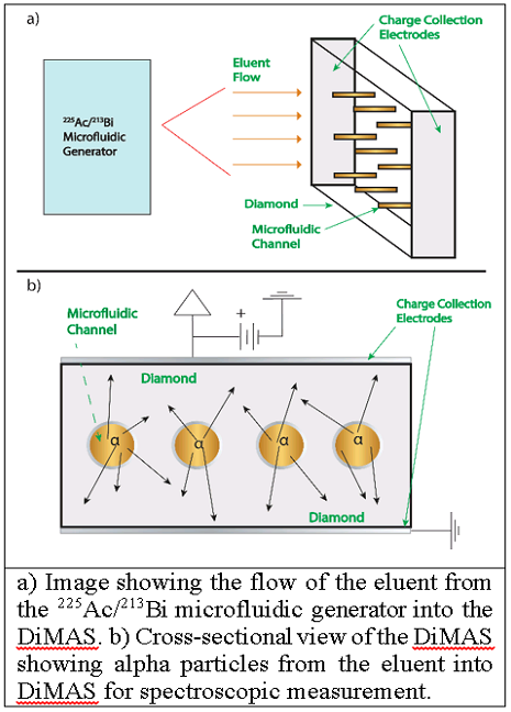 The need to conduct alpha counting and spectroscopy is a desired capability in many fields of science, ranging from radiotherapies to nuclear material processing. Our research group is developing a method to conduct in-line analysis of alpha-emitting isotopes in-solution via microfluidic sensors. The concept relies on the use of narrow channels to limit source self-attenuation in-solution, thereby allowing the spectroscopic measurement of emitted alpha particles, not just total counts. This innovation enables measurement of all alpha-emitting species and removing the background from gamma-rays and beta particles that are inevitably emitted during radioactive decay. In the image provided, a depiction of the application of the diamond-base microfluidic alpha spectrometer (DiMAS) is provided as applied to a Ac-225/Bi-213 cow.
KSr2I5:Eu Scintillator For Nuclear Security
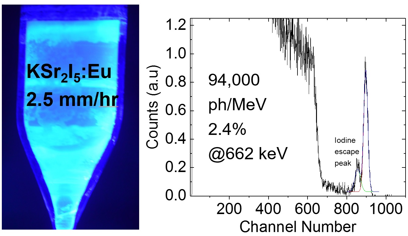 A new class of potassium-containing scintillators has been developed within the Scintillation Materials Research Center (SMRC) that shows excellent linearity and is very bright (near 100,000 photons per MeV). Experimental results have demonstrated an energy resolution approaching 2%, which is considered the holy grail energy resolution for scintillation detectors. Further, the growth of this scintillator has shown to be fast, thereby lowering its cost of prodution compared to other, high resolution scintillators, such as SrI2:Eu. However, the presence of K-40 in the crystal matrix results in an intrinsic radioactivity, which manifests itself in the differential pulse height spectrum. Currently, the Department of Homeland Security's Advanced Research Initiative (ARI) program is funding our group in collaboration with the SMRC to both develop and evaluate the efficacy of these potassium-containing scintillators (e.g., KSr2I5:Eu) for hand-held applications in nuclear security. Our group is currently working on pulse processing designs and algorithms for source detection, identification, and localization in a portable package.
Coded Moderator Fast Neutron Imager
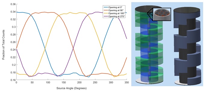 Plutonium-based nuclear weapons emit fast neutrons that can be exploited for their detection and localization. Current techniques utilize advanced imaging systems, such as scatter cameras and coded aperture detection systems. These systems are complex, expensive, and can exhibit a significant time delay in obtaining the necessary certainty in detection/localization of the source. Our research group is currently working on an alternative approach, where a coded moderator is employed to modulate the impinging neutron field to induce a spatially dependent response in inexpensive, thermal neutron-sensitive detectors. This novel design eliminates the need for gamma/neutron discrimination via detector pulse shape (PSD). In the image provided, the sensitivity of one of our cylindrical designs demonstrates the response across the detection system to 1 MeV neutrons equivalent to 8 kg WGPu at a distance of 50 m. The variable height response is a function of the coded moderator, and each curve represents the source-detector orientation. Details on the rectangular design can be found in the associated published article in the Publications tab.
Lithium Indium Diselenide
Lithium indium diselenide (LISe) is a newly discovered I-III-VI semiconductor (sc-LISe) and scintilator (s-LISe) that is highly sensitive to thermal neutrons when enriched in lithium-6. This novel material has opened the door for the development of new, direct conversion thermal and fast neutron sensing technologies. Our group is focusing not only on the application of LISe, but also on understanding its electronic properties. This is vital, because a complete understanding of the signals generated by LISe from all types of ionizing radiation requires knowledge of its semiconducting properties. To this end, we are currently using several techniques to investigate LISe, including transient current analysis, charge collection efficiency, ionic conductivity, and defect characterization techniques.
The application of LISe ranges from area monitoring of thermal neutron fields and the use of themal/fast neutrons for imaging materials. We are currently investigating several potential applications of LISe, but as an example, we will discuss our application of LISe in neutron imaging of materials. Typically, in neutron transmission imaging, scintillation detectors are used, most commonly ZnS:LiF, where the LiF provides the neutron sensitive component. However, ZnS-based imaging systems are limited in their spatial resolution and timing properties. Both semiconducting and scintillating LISe provide the potential to upgrade imaging sensors at neutron imaging facilities. The goal is to simultaneously increase the neutron quantum efficiency (meaning increasing the number of neutrons detected, thereby lowering the required measurement time) and spatial resolution. This project is supported through a subcontract with CNS Y-12 National Security Complex and experimental evaluation is being conducted in the laboratories at the University of Tennessee and at the High Flux Isotope Reactor (HFIR) CG-1D Neutron Imaging Facility at Oak Ridge National Laboratory.
Thermal Neutron Imaging using sc-LISe
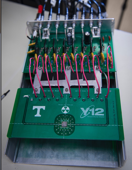
Semiconducting LISe provides the potential for high spatial and temporal resolution neutron imaging. To this end, we have developed a custom LISe 16 channel imaging system to prove the feasibility of such a detection system. Our 16 channel imager is shown in the picture on the right, where we designed the electronics circuit boards and patterned and packaged the LISe sensor in-house. This imager was successfully demonstrated at the CG-1D Neutron Imaging Facility at Oak Ridge National Laboratory. Results indicated that we could successfully image objects with a spatial resolution of several hundred microns. This result is quite promising, since a 16 channel imager is not typically able to image large objects to such a high resolution. The associated publication can be found in the Publications tab. Continuing investigations are underway, where we are coupling sc-LISe to the state-of-the-art Timepix ASIC, developed for particle tracking at the Large Hadron Collider. With a pixel pitch of 55 µm, the sc-LISe neutron imager will provide the highest combination of speed, gamma-ray rejection, spatial resolution, and neutron detection efficiency of any neutron imager commercially available.
Thermal Neutron Imaging using s-LISe
 The optical clarity of s-LISe enables highly efficient neutron detection, where light scattering and diffusion in opuque, polycrystalline materials like ZnS(Cu):LiF neutron converters is a fundamental limitation. Therefore, we have investigated the use of s-LISe for neutron imaging at the CG-1D Neutron Imaging Facility at Oak Ridge National Laboratory. In the rotating image provided, a marmorated stick bug is being radiographed as a function of angle to generate a 3D image of the bug. The investigation considered both reflective and
 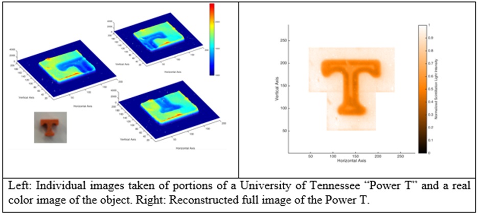 anti-relflective backing on the s-LISe samples to identify its effect of image constrast and resolution. Further, in the Volunteer sprit, we generated a radiograph of a 3D printed Power-T. The excellent neutron absorption properties and intrinsic gamma-ray sensitivity yields many applications of LISe, from hand-held devices to area monitors at neutron-producing facilities, such as a nuclear reactor.
3D Diamond-Based Charged Particle Tracking Detector
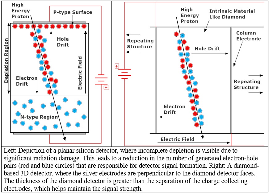 The radiation tolerance of the inner tracking charged particle detectors of ATLAS and CMS at CERN receive a large integrated flux (fluence) of ionizing radiation over their operational lifetime. Silicon-based semiconductor detectors are currently used near the interaction point of ATLAS and CMS. Over the current operational lifetime of the Large Hadron Collider (LHC), many tricks have been played with the silicon sensors to keep them operational after experiencing a large radiation dose. However, current plans to upgrade the LHC for higher luminosity experiments require an even higher radiation tolerance, and silicon sensors are expected to be insufficient after the upgrade. Therefore, a search for alternative radiation sensing technologies is currently underway.
One potential option is the use of semiconducting diamond detectors in a 3D geometry. The "3D" concept of a radiation detector is to use charge collecting electrodes through the semiconductor rather than on its surface, which is how all semiconducting radiation sensors currently operate. Therefore, the 3D design is, in essence, a solid state wire chamber, analogous to gaseous wire chamber detection systems. The benefit of a 3D design is that the distance between electrodes is kept small compared to the sensor thickness, which reduces electron-hole trapping, thereby maintaining signal integrity. A comparison between planar and 3D detector architectures is provided.
All current investigations into 3D diamond detectors utilize pulsed lasers to create graphitic columns in diamond to act as conductive charge collecting electrodes. However, current results indicate that the quality of the conducting wire electrodes are not conductive enough for high-speed, low noise application. Therefore, our research group is investigating the use of scalable micro-fabrication processes commonly used in silicon electronics. The potential benefit of this design is that the fabrication is scalable, utilizes equipment available to many electronic foundaries world-wide, and will produce more conductive wire electrodes in diamond.
